Announcement

Collapse
No announcement yet.

D.I.Y.ตอน เครื่องขยายเสียง

Collapse
X
 
  • Filter
  • Time
  • Show
Clear All
new posts

  • ทดลองทำ 5A. ตัวนี้ดีกว่า.....เน้อ...


    link

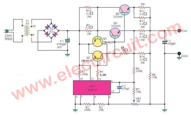
    http://www.eleccircuit.com/regulator...-2n3055-2part/

    ....................

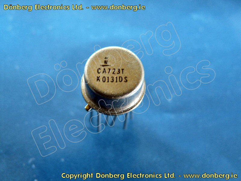
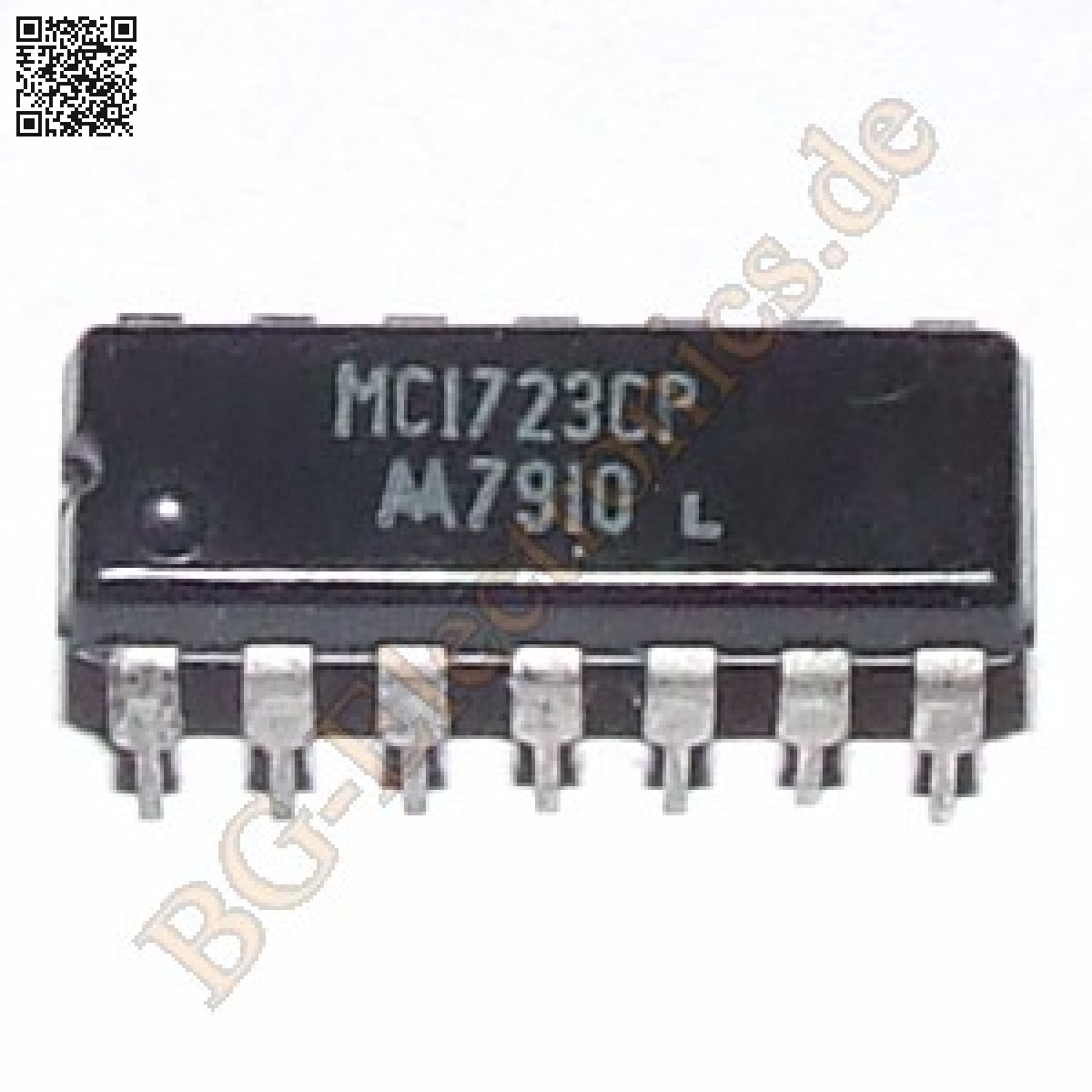
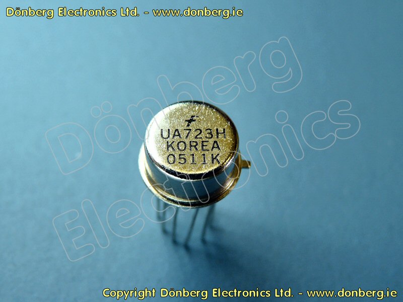
    MC1723 (ON Semiconductor)

    http://doc.chipfind.ru/onsemi/mc1723.htm
    Last edited by jinn; 23 Apr 2012, 14:14:41.

    Comment


    • 723 Shunt Regulator


      -------------------------------------------------


      Last edited by keang; 23 Apr 2012, 19:13:09.

      Comment


      • >>>>>>Build a Low-Voltage Tube Hybrid Headphone/Line Amp<<<<<<<


        http://www.pmillett.com/hybrid_head.htm

        http://www.pmillett.com/file_downloads/ax_hybrid.pdf
        Last edited by jinn; 23 Apr 2012, 19:57:23.

        Comment


        • ไม่รู้...จะรอด มา ได้ฟัง...หรือเปล่า...ตัวนี้

          หลอดมารอแล้ว....อะ่

          Comment


          • คือผมทำตามวงจรในรูปนะครับ ตอนแรกก็เสียงปกติ แต่ผมทำไฟบวกลบชนกันแปปนึง ผมฟังไปได้สักพัก เสียงแตกครับ เปลียน opam แล้วก็ยังแตก พอเล่งโวลุ่มเสียง อื่อดังมากๆๆ และ มีการวู้บ มีเสียงบ้าง วู้บบ้างตอน หมุนวอลุ่ม แตกกระจาย เสียง อื่อๆๆๆๆๆ

            ช่วย แนะนำหน่อยครับว่า อาการน่าจะมาจากครงใหน Untitled.jpg

            Comment


            • kit reg +0- ของprakitแอบมีดีน่ะ
              แกะมาดู ถึงรู้ว่าเขาให้ c nichicon HE กับ rubycon YXF

              Comment


              • เครดิต : Douglas C. Smith
                > High Frequency Measurements Web Page


                February 2000 : Measuring Capacitor Self-inductance and ESR

                Figure 1. Test Circuit for Measurement of Capacitor Self-inductance and ESR


                Technical Background
                The parasitic parameters of a capacitor, that is its equivalent series resistance (ESR) and its inductance, affect the way the capacitor performs in circuits. Some applications are very sensitive to these parameters. For instance, a bypass capacitor used between power and ground in a digital circuit must be able to supply current quickly to nearby active devices. If it has too much inductance it will not be able to do this. Similarly, the transient response of a capacitor used to divert a current pulse due to electrostatic discharge is very important to the ability of the capacitor to do its job.

                So how can the parasitic parameters of a capacitor be measured? One could certainly connect the capacitor to a network analyzer and get a very good characterization. Such an instrument can be quite expensive though. Even the less expensive capacitance measuring instruments may not be available when needed. Both instruments may not provide the information in an easily usable form. If you have a pulse generator (preferably with a 50 Ohm output impedance) and an oscilloscope, you can easily measure the transient response of a capacitor. From this data the capacitor's ESR and inductance can be determined.

                First, construct the simple network shown in Figure 1 at the end of a 50 Ohm coaxial cable fed from a 50 Ohm pulse generator. A 50 Ohm resistor is used in Figure 1 to terminate the coax during the rising edge and provide a total of 100 Ohms of source impedance. The resistor shown is a 51 Ohm 1/2 watt carbon composition resistor with one lead trimmed so that the resistor just seats with the trimmed lead fully inserted into the BNC connector. It may be necessary to put a little solder bump on the resistor lead so that it stays firmly in the BNC connector. The capacitor to be tested is connected between the end of the resistor and the shell of the BNC connector. An oscilloscope is connected directly across the capacitor using leads as short as possible to connect the probe. Probes with a resistive input impedance of 500 to 1000 Ohms are recommended. Standard 10X "Hi-Z" probes often have rising edge effects that will distort the part of the waveform used for the calculations.


                .... ตัดเนื้อหาส่วนของการคำนวนออก แต่ควรเข้าไปอ่านเนื้อหาทั้งหมด ....


                Figure 3 below shows the initial rise from the generator. The black square indicates the vertical voltage and horizontal time scales. The open circuit voltage was a little over 4 Volts with about a 5 nanosecond risetime. The data in Figures 3 through 6 were taken with an analog scope some years ago. Figures 4 through 6 show data obtained from several leaded capacitors (as opposed to surface mount). Two traces were taken for each capacitor. The lower trace was measured at the capacitor body where the leads entered and the upper trace included the minimum amount of lead to practically connect the capacitor to a printed wiring board. The upper trace would not be needed for modern surface mount capacitors unless one wanted to model the connection inductance from the capacitor to the point of interest on a printed wiring board.

                Figure 3. Input From Pulse Generator


                Figure 4 shows data from a 4 uF electrolytic capacitor. The ESR offset is about 50 mV yielding an estimate of the ESR of just over one Ohm. Notice that there appears to be some oscillations on the 1/C part of the slope. This could be scope probe resonance or a resonance in the capacitor. The data was taken with a standard 10X Hi-Z probe, so the probe is suspect. I have seen capacitors with pronounced oscillation from internal resonance. If you are planning to put a large capacitor in parallel with a smaller one, especially if they are constructed from different technologies, it would a good idea to check out the impulse response of the combination using this method. It is possible for the smaller capacitor to resonate with the inductance of the larger one, causing an unexpected result.

                Figure 4. 4uF Capacitor


                Figure 5 shows the result for a 1 uF capacitor of the same construction as the 4 uF capacitor tested in Figure 4. Note that the inductance is similar to the 4 uF capacitor, but the ESR is slightly lower. Since an analog scope was used, the waveform was repetitive and the slight slope on the left half of the waveform was the end of the exponential fall from 5 volts. If a single pulse on a digital scope was used, the slope to the left of the Ldi/dt spike would be zero.

                Figure 5. 1uF Capacitor


                Figure 6 shows the result for a 1 uF radial ceramic capacitor (square case). Note the low inductance and undetectable ESR. Note also that the slope of the 1/C exponential rise is flatter indicating more capacitance than the 1 uF capacitor of Figure 5. This may be due to the fact that the electrolytic capacitor used for Figure 5 may have lower capacitance near zero voltage than at its operating voltage whereas the ceramic capacitor has a more constant capacitance with voltage. The inductance corresponding to the lower trace is estimated to be 4.4 nH.

                Figure 6. 1uF Ceramic Capacitor


                It is interesting to note that a 0.1 uF ceramic capacitor in the same size package as the 1 uF of Figure 6 showed a slightly higher inductance in this test setup. I believe this was due to the fact that the smaller capacitor did not fill the package and internal lead inductance caused the effect. In this case, a 1 uF capacitor was a better choice than a 0.1 uF!

                One of the advantages of this test is that the output waveform is the transient response of the capacitor. The voltages developed across the capacitor in this test are directly related to what will happen in a real circuit if the current risetime from the generator is similar to what the capacitor will see in its intended application.


                --------------------------------------------------------


                December 2011 : Measuring the Resonant Frequencies Of Heat Sink Tines

                ( Your heat sink can be the source of high frequency EMC emissions! )

                Figure 1. Typical Heat Sink


                Abstract :
                Heat sinks on ICs can be a source of emissions at high frequencies in the multi-GHz range. A method of identifying high risk frequencies by measuring the resonant frequencies of the heat sink tines is discussed.

                Discussion :
                Many heat sinks have tines that protrude perpendicularly from a base plate such as the one shown in Figure 1. Today's clock frequencies are so high as to be able to excite the tines as quarter wave monopoles resulting in something like an antenna farm on top of the IC, potentially radiating a clock harmonic or other source resulting in an emissions problem.

                One way to measure the resonant frequency of physical structures in general and heat sink tines in particular is shown in the June 2006 Technical Tidbit, Measuring Structural Resonances on this site. Basically, one would hold a very small shielded loop at the base of one of the heat sink tines to couple energy into the tine. By measuring the reflected signal from the small shielded loop, the resonant frequency of a tine can be measured as the frequency where the reflected signal experiences a dip as the tine absorbs energy from the loop. The lowest frequency this would occur at is the frequency at which the tine is 1/4 wavelength. The method is described in detail in the June 2006 article referenced above. Figure 2 shows the method being applied to a PCB test board mounted over a copper clad board. The object in that case is to measure the resonant frequency of the LC tuned circuit composed of the capacitor formed by the PCB and copper clad board, and the inductance of the short wire between them.

                Figure 2. Use of a Small Shielded Magnetic Loop to Measure PCB-Chassis Resonance


                I observed a case some years ago where 4.7 GHz was leaking out of every slot and seam in the enclosure of a product. It turned out that 4.7 GHz was the third harmonic of the processor clock. When I measured the resonant frequency of the hea tsink tines, the dip in the reflection from the loop was right at 4.7 GHz indicating the tines were 1/4 wavelength monopoles, very efficient radiators, at that frequency. If the tines had been longer or shorter the emissions problem would have been reduced significantly.

                Summary :
                Using the simple method outlined, one can determine the resonant frequencies of the tines on a heat sink. Knowing this information in combination with information about the IC used allows an assessment of the risk of emissions problems from the heat sink.


                --------------------------------------------------------


                September 2011 : PCB-Chassis Ground Connections - Avoiding Pitfalls Due to Unintended System Resonances

                Figure 1. PCB With Chassis Ground Connection


                Abstract :
                PCB to chassis ground connections are often needed in electronic equipment, but if care is not taken, the PCB and the chassis ground structure can become a hi-Q resonant circuit that may cause problems. Background information is given and techniques to avoid problems in designs are discussed.

                Discussion :
                Connecting PCB signal grounds to equipment chassis ground is a common feature in electronic systems although not necessarily done as shown for the experimental board in Figure 1. Problems can arise when the PCB and nearby metal, whether it is another PCB or chassis metal, form a parallel plate capacitor and the connections between them form an inductor. The combination forms a high-Q resonant circuit as illustrated in Figure 2. If this resonant circuit is tuned to a clock harmonic or other critical system frequeny, there is a risk of an EMC problem or even an operational problem for sensitive circuits. At today's frequencies, all PCBs have significant capacitance to nearby metal and all connecting wires are inductors.

                Figure 2. Equivalent Circuit of PCB and Chassis Connections


                Summary :
                Don't take chances with your design, engineer the system resonances involving PCBs rather than letting system performance fall to chance.


                --------------------------------------------------------


                July 2011 : Measuring ESD Stress on a PCB
                ( When Conventional Measurements Don't Work )

                Figure 1. Measured Current Through a Protection Device on a PCB
                ( Vertical Scale = 50 mA/div, Horizontal Scale = 20 ns/div )


                Abstract :
                Measuring voltage stress on components on a PCB under ESD conditions can be difficult as the ESD noise can inject error in the measurement. Often this error is larger than the voltage of the stress to be measured. A method of measuring voltage stress is discussed that has very high common mode rejection and low ESD induced error.

                Discussion :
                ESD induced error makes accurately measuring voltage stresses on a PCB difficult. In addition to high common mode noise, high amplitude time varying electric and magnetic fields can introduce error in the measurement loop formed by the voltage probe and the nodes to be measured unless this loop is kept very small. One way to accurately measure high frequency voltage stress is to replace the component that is being stressed, such as an IC, with a TVS or similar protector connected across the two nodes to be measured. In series with the protector, form a loop as small as possible to insert a current probe to measure the current through the protector.

                As the ESD or other pulsed voltage stress is increased, an increase in current through the parasitic capacitance of the protector will be seen that follows the stress applied. When the breakdown voltage of the protector is reached, additional increase in current may be noted and the waveform will quickly show the current waveform as the stress is increased further for a protector that clamps to a specified value. For a protector that latches to nearly a short after turn-on, like an SCR, the current at the point of latching will be seen. Figure 1 shows the current through a protector that clamps to a specified voltage in a circuit with applied stress from a Fischer Custom Communications model TG-EFT high voltage pulser. The protector capacitance is helping form a resonant response with circuit inductance. The current waveform reaches a peak of about 80 mA.

                In Figure 2, the stress is doubled and the peak current reaches about 150-160 mA, approximately increasing linearly with applied stress and keeping the same waveshape except the ringing frequency is slightly higher.

                Figure 2. Measured Current Through Protection Device on a PCB at 2X Applied Stress
                ( Vertical Scale = 50 mA/div, Horizontal Scale = 20 ns/div )


                For Figure 3, the stress is increased to 3X the value in Figure 1. Note that the waveshape is beginning to change although the peak current is about 3X of the current in Figure 1, about 230 mA.

                Figure 3. Measured Current Through Protection Device on a PCB at 3X Applied Stress
                ( Vertical Scale = 50 mA/div, Horizontal Scale = 20 ns/div )


                In Figure 4, the stress is increased to 4X the value in Figure 1. Now the waveshape is definitely changed and is beginning to look like the current waveform I expect at this point in the circuit. The peak current is now almost 300 mA.

                Figure 4. Measured Current Through Protection Device on a PCB at 4X Applied Stress
                ( Vertical Scale = 50 mA/div, Horizontal Scale = 20 ns/div )


                The stress that just begins to breakdown the protector is that of Figure 3 where the waveshape begins to change. Note that we are not trying to accurately measure the current, so some electric field response of the current probe is acceptable, we are looking for a change in the waveshape of the current as the stress increases. The current probe should be as small as possible so as to minimize the loop needed to insert it into the circuit.

                The lower capacitance the protector has before breakdown, the larger the difference in amplitude and waveshape will be noted at the point of breakdown. Also, if the capacitance of the protector is much larger than the original device it replaced, the capacitance may reduce the voltage across the protector resulting in a larger applied stress being required to breakdown the protector. This will result in measurement error that will understate the stress on the original device to be measured. In general, the lower capacitance the protector has the better, but for sure it should not be much larger than the original device it replaces in the circuit.

                Summary :
                Using a current probe and a protector connected in place of a device on a PCB to measure voltage stress on the device is a useful way to minimize error from sources like ESD in the voltage stress measurement. The capacitance of the protector used should be minimized and be on the order of the original device capactiance. The loop formed for the current probe should be as small as possible.


                --------------------------------------------------------


                August 2009 : The Square Shielded Loop - Part 6, Measurements in the Time Domain Using a Comb Generator
                ( An unusual use for a comb generator )

                Figure 1. A Shielded Loop Being Used to Sense Signal Current from a Comb Generator


                Abstract :
                Possible sensitivity to electric fields/capacitive pickup has been a factor in the past in selecting shielded magnetic loops over unshielded ones. Data is presented to show that in the near field, shielded loops may be required for sensing signal currents in some cases. Data presented in prior Technical Tidbits have shown the opposite to be true for other cases.

                Discussion :
                Figure 1 shows a shielded magnetic loop probe held near a ground plane split to sense signal current. Probe construction is shown in the cutaway view of Figure 2. A section of semi-rigid coax is shorted at it's end and then bent around and the shorted end is soldered onto the coax to make a loop. A small gap is cut in the shield to permit the loop to be sensitive to magnetic fields. In Figure 2, the shield gap can be seen at the midpoint of the rightmost side of the loop, opposite the soldered junction.

                Figure 2. Construction of a Square Shielded Loop


                Data was also taken using the unshielded wire loop shown in Figure 3 to compare the responses of the two magnetic loops and determine when the wire loop's electric field sensitivity becomes important.

                Figure 3. A Simple Wire Loop


                The signal source, shown in Figure 4, for this experiment was an AET USB Powered Comb Generator. Comb generators produce a large number of harmonics that are useful in a number of frequency domain measurements normally made using a spectrum analyzer or similar instrument. But in this case, it was used to furnish fast pulses for the experiment and measurements were made on an oscilloscope. The comb generator used has a 1.8 MHz fundamental frequency and edge rates of about 400 picoseconds.

                The output of the comb generator was connected to the BNC connector in the upper left corner of the circuit board in Figure 1. The resulting current in the signal path and the load resistor on the right side of the board resulted in signal current flowing around the split in the ground plane and both shielded and unshielded loops were used to sense this current.

                Figure 4. AET USB Powered USB Comb Generator


                Figure 5 shows the test setup using the simple wire loop of Figure 3. This is the same setup shown in Figure 1 for the shielded loop except for the use of the unshielded loop.

                Figure 5. Test setup with unshielded wire loop


                Figure 6 shows the output of the shielded loop. A resonance at about one GHz can be seen on the waveform. This could be partially due to loop self resonance or capacitive coupling to the shield. To test the effects of electric field coupling, the loop was rotated by 180 degrees. The inductive pickup should invert and any capacitive pickup should stay nearly the same. The reversed loop output is shown in Figure 7 and is just an inverted version of the wave shape in Figure 6. Since the waveforms in Figure 6 and Figure 7 are inverted with otherwise the same shape, capacitive coupling to the loop is not significant for this configuration.

                Figure 6. Output from shielded loop
                ( vertical scale = 10 mV/div, horizontal scale = 2 ns/div )


                Figure 7. Output from shielded loop - reversed orientation
                ( vertical scale = 10 mV/div, horizontal scale = 2 ns/div )


                Figures 8 and 9 show the same cases for the unshielded wire loop. One can easily see these waveforms are not just inverted versions of each other. There is significant capacitive coupling between the loop and the circuit. The capacitive coupling combined with the inductance of the wire probably produced the lower frequency resonance easily seen in Figure 9 and to a lesser extend in Figure 8.

                Figure 8. Output from wire loop
                ( vertical scale = 10 mV/div, horizontal scale = 2 ns/div )


                Figure 9. Output from wire loop - reversed orientation
                (vertical scale = 10 mV/div, horizontal scale = 2 ns/div)


                I encourage you to read the other five Technical Tidbits in the "Square Shielded Loop" series. These are linked just below the summary paragraph. In the September 2008 Technical Tidbit, "The Square Shielded Loop - Part 5," the unshielded wire loop was used for signal injection of pulses with a 2 ns edge rate. A significant capacitive effect was not present. If fact, for injecting signals into the board of Figure 1 over the ground split parallel to the signal path, the simple wire loop worked better than the shielded loop, having a flatter frequency response. In that case, the shield of the loop formed a parasitic resonant circuit with the circuit board that affected the frequency response of the coupling from the loop to the board.

                Summary :
                Significant capacitive coupling was demonstrated when using an unshielded wire loop to sense current flowing near a ground plane split. Yet, other Technical Tidbits in the "Square Shielded Loop" series show that for injecting a signal into a signal path crossing a ground break, the simple wire loop was superior. Until more work is done, one must test to see which type of loop works best for a given situation and not just assume that one type of loop is always better.


                --------------------------------------------------------


                April 2010 : Identifying Switching Power Supply Noise in Systems
                ( Frequency Domain Measurements )

                Figure 1. Test Setup For Measuring Switching Power Supply Induced Noise Current into a Nearby Wire
                ( Spectrum Analyzer Screen at 10 dB/div Vertically and 10 MHz/div Horizontally )


                Abstract :
                Switched mode power supplies can generate significant harmonics of such an amplitude as to cause EMC emissions problems in the 30 to 100 MHz range and occasionally at higher frequencies. Identifying switching power supply noise is discussed as well as one coupling method that can result in excess radiated emissions.

                Discussion :
                Figure 1 shows the test setup used to generate the data. The setup is composed of a switching power supply, a (black) wire draped across the supply, an Agilent N9320B spectrum analyzer, and an Fischer F-33-1 current probe. The power supply is powering a 48 Watt, 12 Volt incandescent light bulb through the yellow test leads. The black wire passing through the F-33-1 current probe is about three meters long and its center has been positioned over the power supply. The plot on the analyzer screen in Figure 1 extends from zero Hz to 100 MHz at 10 MHz/div.

                The noise floor on the screen of the analyzer is about 30 dBuV, a level that corresponds to enough current flowing in a one half wavelength dipole antenna to just hit the CISPR/FCC class B emissions limits in the 30 to 100 MHz frequency range. You can see the level of current near 40 MHz is about 20 dB above that level and could cause a Class B emissions problem. In reality, the power supply exhibits broad band noise, but the current in the wire peaks at the frequency at which the wire is a one half wavelength dipole. At that frequency, the driving point impedance of a dipole is near 70 Ohms, its minimum value, and the induced voltage from the power supply in the black wire is able to produce a current maximum at the center the wire.

                The local field from the power supply is probably not physically large enough to radiate efficiently at 40 MHz, but once it induces enough current in the nearby black wire, the wire itself is long enough to be an efficient radiator. That is what has happened in this case.

                We know that the source is the power supply for this simple case, but in some cases the source might not be so obvious. One way to discover if a broadband noise, such as shown on the analyzer screen in Figure 1, is due to a switching power supply is to adjust the analyzer as shown in Figure 2.

                Figure 2. Spectrum Analyzer Screen Centered at 43.5 MHz with a 100 kHz/div Horixontal Scale and a Resolution Bandwidth of 1 kHz


                The analyzer has been adjusted in Figure 2 to focus the plot around a center frequency of 43.5 MHz with a frequency span of only one MHz, 100 kHz/div. The resolution bandwidth has also been lowered from 100 kHz in Figure 1 down to one kHz, a value consistent with the horizontal scale of 100 kHz/div. With these analyzer parameters, you can clearly see peaks in Figure 2 separated by about 120 kHz, the fundamental frequency of the switching power supply used for this experiment.

                Noise originating in switching power supplies that operate at a constant frequency will produce a spectrum plot similar to Figure 2, although the spacing of the harmonics may be different. That the noise is actually coming from a specific supply can be determined by holding a small loop probe near the power supply to pick up induced noise. Display the loop output on an oscilloscope or spectrum analyzer to determine the fundamental frequency. If the observed noise has a harmonic spacing the same as the fundamental switching frequency of the power supply, the supply is the likely source of the noise unless there are other supplies in the system with "the same" fundamental frequency. For the case where there are several power supplies with "the same" fundamental frequency, they are likely slightly different and this information can be used to narrow the source of the noise down to one supply out of several.

                Summary :
                By expanding the spectrum plot of a broadband noise, individual harmonics from the source of the noise can be resolved. In many cases, the spacing of harmonics on the expanded plot will identify a switching power supply as the source of the noise.

                Comment


                • ผมมีหม้อแปลง 12-0 จะต่อไดโอด (DIODE) ยังไงให้ไฟออกเป็น 12+ 0 12- ครับ

                  Comment


                  • ผมต่อแบบนี้อ่ะ

                    Comment


                    • กำลังจะทำลำโพงแบกไปฟังที่อื่นได้ครับ


                      ic 2005r สองตัว ลำโพง4 เดียวเป็นรูปเป็นร่างจะถ่ายรูปมาให้ดูตอนนี้กำลังคิดอยู่ว่าจะใช้แบต C size 8ก้อน หรือจะหาซื้อแบต UPS สักลูก ถ้าC 8ก้อนข้อดีคือมีรังถ่านมาให้อยู่แล้ว


                      ถอดไปล้าง อายุน่าจะมากกว่าผมส่วนวงจรเดิมก็อยากซ่อมน่ะครับแต่วงจรน่ากลัวมาก ในของค่อนข้างดี c สภาพภายนอกปกติดีทุกอย่าง ตกใจมากคิดว่าคงมีบวมๆบางและ
                      คืบหน้าอย่างไรจะมาบอกกล่าวครับ

                      Comment


                      • ไม่แน่ใจน่ะ แต่หม้อแปลงไม่มีcenter tab จะเอาไฟ +0- ผมว่ามันต้องทำvirtual groundน่ะ ไม่งั้นอาจจะต้องใช้วงจรสวิทชิ่งช่วย
                        ไปหาหม้อแปลงมีcenter tabน่าจะง่ายกว่า

                        --------


                        emitter follower single end ไว้ใช้แทนbuf 634 ในแอมป์หูฟัง
                        ตัวจริงเสียบแทนbuf634ได้เลย


                        schematicสำหรับคงอยากลอง

                        บอกไว้ก่อนว่าbias กระแส คำนวณมั่วหน่อยน่ะ ไม่ชัวร์เท่าไร
                        ไม่ได้bias เยอะ ไม่มีที่ให้ใส่ซิงค์สำหรับtr
                        ใครอยากทำตามแล้วใส่ซิงค์ได้ ก็ลองลดค่าความต้านเพิ่มค่าทนวัตต์Rลงไปอีกดู
                        ค่าRที่ในวงเล็บ คือค่า ที่ใช้จริง ใช้กับไฟ+-12v ถ้าไฟมากน้อยกว่านี้ก็ลด หรือเพิ่มตามโวลท์มันเอา
                        ไม่อยากใช้ตัวใหญ่ ทนวัตต์มาก ก็เอาตัวทนวัตต์น้อยมาอนุกรม-ขนานให้ได้ค่าใกล้เคียง ให้มันเฉลี่ยpower dissipation กันไป

                        edit : ถ้าเอาไปใช้ ตัวมันควรอยู่ในfeedback loop

                        --------


                        ตอบพี่เสื่อ rep ล่าง ขอไม่ขึ้นโพสต์ใหม่น่ะ รีวิวเสียงมันจะได้อยู่ในโพสต์เดียวกัน

                        เอาแบบคร่าวๆน่ะ ยังไม่เทสละเอียด เทียบกับbuf634
                        emitter follower ชิ้นเสียงออกใหญ่กว่า imageเสียงบางเสียงจะฟังดูกล้วงๆ กว่าหน่อย (จุดอ่อนมันเลยล่ะ)
                        หัวเสียงไม่กระทุ้งกระแทกแบบbuf634 หางเสียงเก็บตัวช้ากว่า
                        มิติด้านสูงดีกว่า เสียงกลาง-เสียงร้องหนากว่านิด เสียงเครื่องดนตรีบางชิ้นถอยหน่อย(บอกไม่ถูกว่าความถี่ช่วงไหน)
                        ปริมาณเสียงแหลมช่วงบนที่แทงๆ หูหน่อยจะน้อยกว่า

                        สรุป ฟังง่าย ผ่อนคลายกว่าbuf634 ส่วนค่อนข้างชอบ
                        ขนาดbiasไปน้อยน่ะ แถมวงจรเดิมก็ไม่ได้จัดวางให้เหมาะกับมันมากเท่าไร

                        เป็นเหตุให้นั่งวาด ลายทองแดง ของตัวในโพสต์40
                        http://www.overclockzone.com/forums/...1#post40232862


                        vvvvvvv
                        Last edited by ManiacMaew; 30 Apr 2012, 02:27:08.

                        Comment


                        • ทำแล้ว...เสียงเป็นไงบ้างครับ

                          Comment


                          • ตอบไปในโพสต์นั้นแล้วน่ะครับ

                            Comment


                            • @ManiacMeaw
                              ถ้าไบแอสนี้ขยาย Ampitude ของคลื่นเสียงใช่ไหมครับ?

                              ------------

                              TDA2005r วงจรที่สอง


                              อันนี้คือวงจรkit ยัดลงไปเรียบร้อยแล้ว ปล.ใช้ชุดจ่ายไฟชุดเดียว เพราะวงจร peak สุดๆที่วัดได้แค่ 150mA ยังไงหม้อแปลงกับ IC7812 ก็เหลือๆ แค่ต้องให้ C ค่าสูงช่วยตอนดึงโหลด

                              //เท่าที่สังเกต เสียงต่ำมันดึงกระแสสูงกว่าเสียงสูง

                              Comment


                              • Originally posted by pluanant View Post
                                @ManiacMeaw
                                ถ้าไบแอสนี้ขยาย Ampitude ของคลื่นเสียงใช่ไหมครับ?
                                ขยายกระแส ไม่ขยายโวลท์ คือมันไม่มีgain

                                tr เปลี่ยนได้น่ะ npnเบอร์อื่นก็ได้
                                ค่าประมาณๆ ของtr
                                Ic มากกว่า0.5A (0.25 ก็น่าจะพอแล้ว แต่ก็เพื่อไป กระแสที่จ่ายยังไงก็ไปตันที่R out put+ โอหฺ์มหูฟัง) hFE หลักร้อยก็พอ Vce >30volt
                                2n2222 แบบที่คุณkeangเคยบอกไว้ก็น่าลอง
                                Last edited by ManiacMaew; 28 Apr 2012, 21:04:04.

                                Comment

                                Working...
                                X